We think of material synthesis the way our ancestors thought of metalworking: apply heat until something transforms. The blacksmith’s forge, the furnace that grows crystals, the oven that bakes semiconductor layers—all rely on temperature to jostle atoms into new arrangements. But what if you could do the same thing with the press of a point? What if, instead of fire, all you needed was force?
A preprint (arXiv:2606.03710) from a team spanning the University of Pennsylvania, Princeton University, and Zhejiang University suggests exactly that. Led by Robert W. Carpick at Penn, the researchers have demonstrated that the localized pressure of an atomic force microscope tip can write atomically thin patterns of a superconducting material—metallizing a two-dimensional semiconductor one line at a time, at a resolution of about 50 nanometers, at temperatures barely above room temperature. The result is a new, generalizable paradigm for synthesizing quantum materials through mechanical energy alone.
The Point That Draws Atoms
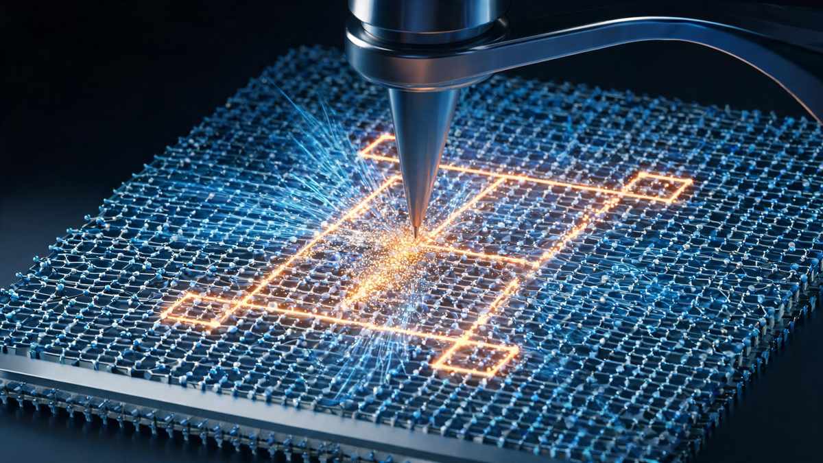
The experiment sounds deceptively simple. The team started with a bilayer of molybdenum ditelluride (MoTe₂), a semiconductor in the family of transition-metal dichalcogenides, capped and placed over a thin strip of palladium. Above it all, the sharp tip of an atomic force microscope (AFM) scanned across the surface in contact mode—a point no wider than about a thousand atoms, pressing down with forces measured in nanonewtons.
Think of the AFM tip as a pen, but a pen that doesn't deposit ink. Instead, the mere pressure of its stroke draws atoms from a buried source into the host crystal. As the tip traced its path, palladium atoms from the underlying strip were pulled into the MoTe₂ lattice, converting the semiconductor patch beneath the tip into a uniform intermetallic compound: Pd₇MoTe₂. The tip wasn't writing with ink; it was coaxing chemistry into being through stress alone—the heat only helping to speed what pressure had already made possible. Unlike a literal pen, however, the atoms didn’t collect on the surface—they diffused into the crystal’s interior, as if the tip’s push squeezed the palladium upward like a syringe drawing medicine from a vial.
The resemblance to calligraphy is more than poetic. By programming the tip’s trajectory, the researchers could draw arbitrary patterns—a Hall bar, for example—writing functional superconducting wires only a few dozen nanometers wide. The spatial resolution was 50 nanometers, roughly a thousand atoms lined up side by side. The act of mechanical writing was not just chemical; it was architectural.
How Force Replaces Heat
The real surprise lies in the kinetics. Chemical reactions, including the diffusion of metals into a host lattice, normally demand thermal activation—the random kicks of hot atoms. To form Pd₇MoTe₂ by heating alone would require temperatures around 200 °C. Yet the team found that applying a normal load of hundreds of nanonewtons could trigger the same growth at near-room temperature—as low as 40 °C. This is not will, but a direct consequence of how mechanical stress alters the energy landscape.
The team mapped this quantitatively. The growth rate of the intermetallic compound increased exponentially with applied force, following Eyring’s stress-assisted thermal activation model, a framework that describes how mechanical energy shifts the energy barrier for atomic rearrangement. They measured the growth rate under varying temperatures and loads, and the data fell neatly onto lines when plotted as the logarithm of rate versus inverse temperature—a telltale signature of thermally activated processes, but with the activation energy itself reduced by the applied pressure. The tip’s push did not eliminate the need for thermal energy; it lowered the mountain that atoms had to climb.
Finite element simulations confirmed the picture. The tip’s compression generated tensile strain in the MoTe₂ layers below, stretching the lattice and making it more receptive to palladium atoms. Density functional theory and ab initio grand canonical Monte Carlo calculations then showed that the strained MoTe₂ sites favored the chemisorption of palladium, driving the formation of the stable Pd₇MoTe₂ phase. It’s as if the tip’s pressure opened a gate, and the thermal jostling of atoms then poured through like water finding a lowered channel.
The effect is a kind of mechanical catalysis. The force doesn’t directly supply the atoms with the energy to move; rather, it reshapes the playing field so that ordinary thermal motion becomes much more effective. It’s like lowering the net in a game of tennis—the players don’t hit any harder, but suddenly many more shots clear the net. This is not a metaphor; it is precisely how stress-assisted kinetics operate.
Drawing Superconductivity
The most striking moment in the paper comes when the researchers characterize what they have written. The Pd₇MoTe₂ is not just a metal; it is a superconductor. The team’s transport measurements on the Hall bar pattern showed a vanishing electrical resistance at low temperatures. Mechanical force, guided by a tiny probe, had drawn a quantum material into existence.
There is something almost alchemical about this. We are accustomed to the idea that exotic quantum states require elaborate crystal growth, epitaxial deposition under ultra-high vacuum, or precisely controlled furnaces. Yet here, at room temperature, with nothing more than pressure and the right starting materials, a tip scribed a path where electrons later flowed without resistance. Of course, the tip doesn’t know it’s writing a quantum state. It simply pushes atoms into place, and the atoms, given the right arrangement, spontaneously decide to conduct electricity without dissipation. The emergence of superconductivity is not a choice made by the experimenter; it is a property latent in the crystal structure, one that mechanical force merely unveiled.
The philosophical implications are subtle but far-reaching. For decades, we have divided synthesis methods into thermal equilibrium routes and energetic deposition techniques. Mechanical force was relegated to a crude role—grinding, indentation, wear. This work forces us to rethink that hierarchy. The same localized stress that can damage a material can, under the right conditions, craft a new quantum phase. The boundary between fabrication and destruction becomes porous; what matters is not the force itself but the chemical environment it encounters. As Carpick and his collaborators show, stress can be as precise a synthetic tool as temperature or electric fields, and with nanoscale resolution that rivals the best lithography.
A New Kind of Pen
Where does this lead? The team proposes that their “mechanochemical nano-writing” is a generalizable paradigm. If the combination of stress and a suitable source material can drive intercalation and phase conversion in MoTe₂, the same principle might apply to other van der Waals materials and other source metals, opening a library of atomically thin quantum materials written by design.
The practical vision is tantalizing: a scanning probe that not only images surfaces but actively crafts them, building superconducting circuits, magnetic patterns, or topological islands with a stroke of the tip. Such a tool would blur the line between synthesis and patterning, between chemistry and device fabrication. You wouldn’t need to grow a wafer of the desired material and then etch away the unwanted parts; you would write the device directly, atom by atom, line by line, like an artist’s brush painting a circuit. This is not will, but the inevitable result of a physical principle: force can be chemistry, and chemistry can be architecture.
The road ahead is not without its potholes. The current demonstration uses a single material system and a single source metal. Whether other dichalcogenides, other intercalants, or other crystal structures can be written with comparable fidelity remains to be seen. Scaling from a single laboratory tip to a manufacturing process is another leap, though parallelized probe arrays are already under development for data storage. The authors also acknowledge that the mechanism hinges on the right balance of strain and chemical affinity; not every combination will yield a stable ordered compound. Yet the direction is clear, and the proof of principle is luminous.
It’s worth pausing to consider what this inversion of thermal synthesis means for our understanding of materials themselves. For centuries, we have treated temperature as the universal dial of transformation: hotter means faster, and the highest temperatures unlock the most exotic states. This work places mechanical energy on an equal footing. It suggests that the energy landscape of chemical reactions is not a fixed terrain but a fabric that can be stretched and reshaped by local stress. The pen that writes superconductivity doesn't burn its way through matter; it persuades matter to become something new, gently, at the smallest scales.
We are left with a question that feels less like a technical hurdle and more like an invitation. What else can be written with such a point? Could we inscribe magnetic domains, quantum spin liquids, or even more exotic topological states? Could the same tip that wrote a superconducting wire one day sketch out a qubit? The answers are not in this paper, but the paper gives us the grammar to ask the questions in a new way. It replaces the blacksmith’s hammer with the calligrapher’s brush, and in doing so, it reminds us that sometimes the most powerful transformation comes not from fierce heat but from the quiet, persistent pressure of a well-placed point.
References
- Shuai Zhang et al., Mechanochemical Nano-Writing of an Atomically Thin Metal, arXiv:2606.03710